
Silicon wafers are produced as part of the development process of your custom ASIC. This takes up to 3 months. Each additional design iteration requires this time-consuming step. Therefore, the number of design iterations, or so called “respins,” needs to be minimised to reduce costs and meet project timing.
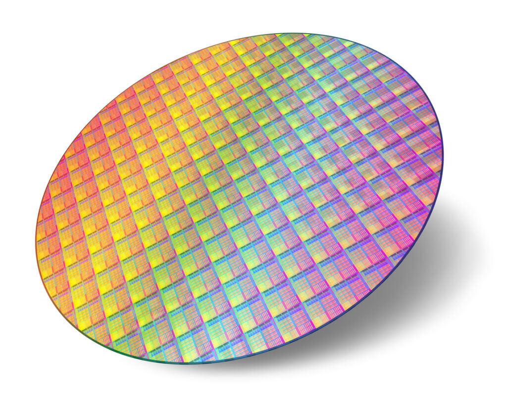
Functional Silicon from the initial prototype run
Typical wafer fabrication takes around 3 months. Less iterations means reduced time-to-market and lower investment.
From the first ASIC prototypes, ICsense guarantees 100% functional silicon, ready for your demo purposes. We have developed a unique design environment to drastically reduce the number of respins.
Since its start, ICsense has reached mass production in all its designs with just 1 iteration, providing our customers with fast time-to-market and projects within budget.
At the core of our comprehensive and unique design environment are known industry tools from Cadence and Synopsys. To increase design efficiency, we built an abstraction layer around these tools along with a requirements management system to further de-risk the development process.
Traditional IC design is largely manual
To understand the power of the ICsense design environment, let’s first have a look at a traditional flow for IC design. This includes:
- Manual sizing of transistors and building blocks.
- Manual control of simulation test benches.
- Manual checking of compliance with the target specification.
- Manual input in a requirements database.
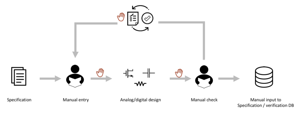
This time-consuming process is prone to human error, outdated parameters, and increases the amount of design iterations. To overcome these risks, ICsense created a unique design flow that meets the toughest project requirements in safety critical automotive and medical design.
ICsense’s unique design approach
In traditional IC design, the designer uses a graphical GUI inside the design software. Transistor sizing, control of parameters and corner settings are all manually set and updated as the design progresses, which is inefficient. Therefore, first of all, we parametrize every circuit and test bench. With embedded design plans we can automate transistor sizing, to make more time for performance improvements.
Our design plans enforce
- a systematic design approach,
- traceability of design choices, and
- efficient porting to future technology nodes.
Embedded requirements management
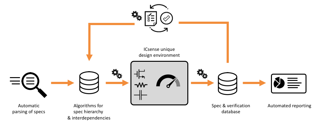
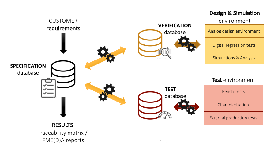
Secondly, our unique RMS, Requirement Management System, is embedded in this design environment to enable real-time consistency with the latest spec version. This system ensures full compliance and test coverage. It enables forward and backward traceability of the specifications as required by ISO26262 automotive functional safety and ISO 13485 medical standards.
Thirdly, after manufacturing the test and characterisation results are automatically verified against the requirements. The platform traces customer requirements and its verification from concept to production, through the whole ASIC life cycle in a systematic and efficient way. It automatically links specifications to their corresponding verification plan, simulation, and bench tests results.
Since 2004, ICsense has designed many first-of-a-kind ASICs and has enabled customers around the globe to outperform their competitors. We specialize in low-risk analog, mixed-signal, and high-voltage ASIC developments. Contact us today for your next ASIC design and supply project.