Home - What we offer - ASIC Design and Supply
Developing a custom ASIC -tailored to your application- can uplift your product and set you apart from the competition. At ICsense, we specialize in designing and delivering the right ASIC solution to power your next innovation. ICsense offers the complete flow from concept, design through mass production of your custom ASIC across the spectrum of sensor/MEMS interfacing, high-voltage, power and battery management, communication, and ultra-low-power ASIC designs.
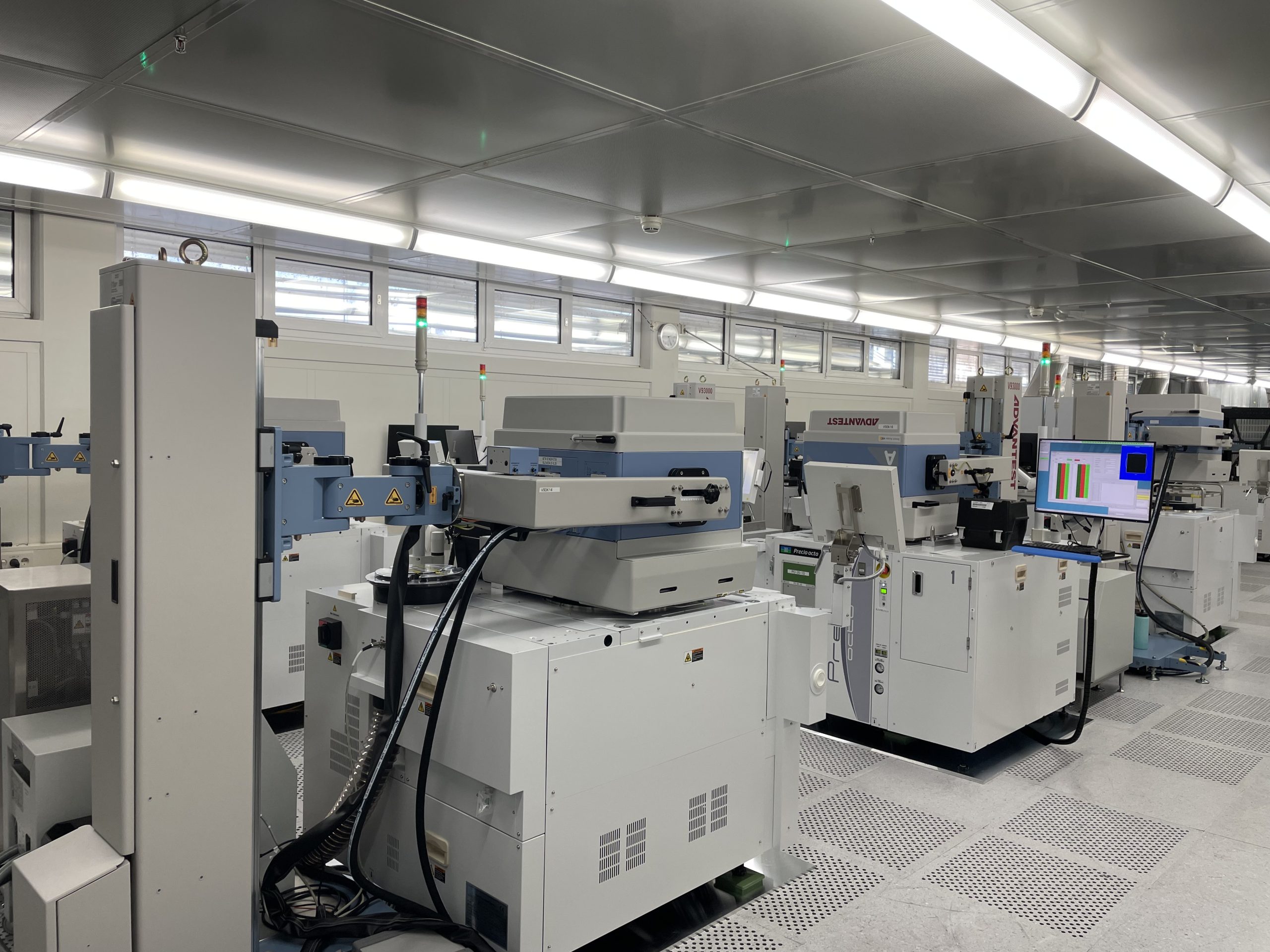
Our end-to-end, one-stop-shop service is designed to unburden you and provide the best possible custom ASIC solution. With in-house design teams, in-house ATE testing, and a strong network of partners and foundries, we seamlessly integrate all the key ingredients to develop a successful ASIC—branded with your name.

"We build longterm relationships with our customers by supplying innovative and cost effective ASICs to support their product roadmap."
ICsense CEO, Bram De Muer


Silicon wafers are produced as part of the development process of your custom ASIC. This takes up to 3 months. Each additional design iteration requires this time-consuming step. Therefore, the number of design iterations, or so-called “respins,” needs to be minimised to reduce costs and meet project timing. Since its start, ICsense has reached mass production in all its designs with just 1 iteration, providing our customers with fast time-to-market and projects within budget.

“As a fabless designer and producer of high memory passive RFID tags, Tego partners with skilled, innovative IC design firms that achieve excellence in their ASIC designs and at the system level. With ICsense, we found such a partner for the development of our RF front-end. Their high quality of service, innovation, IC knowledge and dedication has been instrumental to our success to date. We look forward to continued success with ICsense as a key technology partner for the foreseeable future.”

”ICsense’s expertise in making high-voltage circuits with low-voltage transistors led to first silicon success for this complex and innovative design. We particularly appreciate our close cooperation with ICsense’s engineers and their proactive and flexible attitude.”

”ICsense is one of our major outsource partners to develop large IP blocks to our requirements. We especially value them for their strong technical engagement, robust management, track record of on-time delivery, high-integrity people and their relax company culture.”

“Based on the excellent project track record of ICsense, ON has selected ICsense as one of its preferred IC design partners for analog, mixed-signal and high-voltage. In the numerous projects with different BUs, ICsense has proven to deliver high-quality and reliable IC designs compliant with our stringent demands.”

”ICsense developed the analog front-end for our new industrial transceiver in TSMC 40nm. ICsense is a valuable partner for Renesas and we highly appreciated the flexibility, expertise and innovativeness of ICsense.”

“The flexible attitude of the ICsense design team combined with their advanced analog IC design expertise, specifically for high voltages, significantly impacted the feasibility and the successful integration of our Cochlear implant IC. “

“ICsense developed this first-of-a-kind and innovative ASIC for stimulation and measurement in our 40-electrode deep brain implant. Next to the high technical and quality standards that ICsense employs, we strongly appreciate their open, honest and flexible way of working, which was key to the success of this development.”